RFSoC Loop Back Tutorial
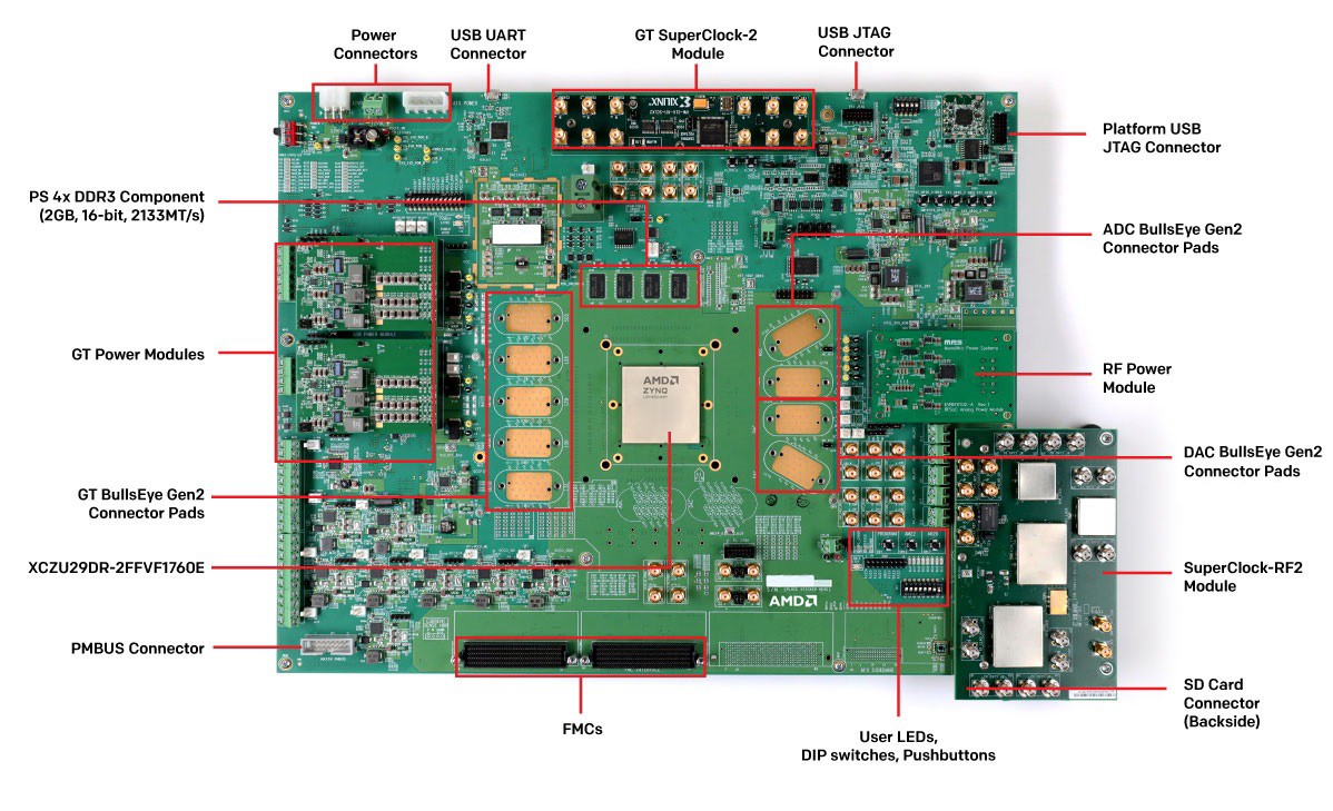
Figure 1: Zynq UltraScale+ RFSoC 1275 Characterization Kit
RF Data Converter IP
Each RFSoC offers multiple RF-ADCs and RF-DACs which are high precision, high speed, and power efficient. Xilinx Vivado is equipped with RF Data Converter IP core which provides a configurable wrapper that allows these RF-ADCs and RF-DACs blocks to be used in the IP integrator designs. The RF-ADCs and RF-DACs are organized into tiles where each tiles contains one, two or four RF-ADCs and RF-DACs. For Zynq UltraScale+ RFSoC 1275 characterization board each tile contains two RF-ADCs and RF-DACs. User can manually alter the power efficient digital down converters (DDCs) and digital up converters (DUCs) that include programmable interpolation and decimation rates. Each tile includes a block with a PLL and all the necessary clock handling logic.
ADC to DAC Loop Back Design Using RF Analyzer
In this section, we will configure the RF data converter IP with user defined specifications and create an example design to understand and familiarize with the board and RF analyzer.
ADC Tile Settings
Figure 2 shows the RF Data Converter IP. Under Basic tab select RF-ADC. For our board we have four ADC and DAC tile each with two pairs of ADCs and DACs. For the example design we will be activating one RF-ADC and RF-DAC channel where we will enable all the pairs of ADCs and DACs in each tile. Even though we will use only ADC 0 and DAC 0 for our loop back design.
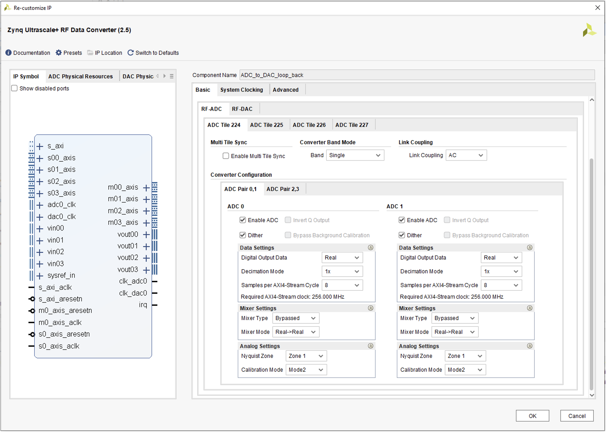
Figure 2: RF Data Converter ADC Tile
From Figure 2, select ADC Tile 224 and enable ADC 0 by checking the Enable ADC check box. This will enable the ADC for the design and similarly we can enable ADCs or DACs that are required.
Data Settings:
- Digital Output Data = Real
- Decimation Mode = 1x
- Samples per AXI4-Stream Cycle = 8
Required AXI4-Stream clock: 256MHz (will automatically be generated based on the system clock that is chosen for the ADC tile)
Mixer Settings:
- Mixer Type = Bypassed
- Mixer Mode = Real -> Real
Analog Settings:
- Nyquist Zone = Zone 1
- Calibration Mode = Mode2
Apply the same settings for ADC Pair 0,1 and ADC Pair 2,3.
DAC Tile Settings
Figure 3 shows the DAC tile settings.
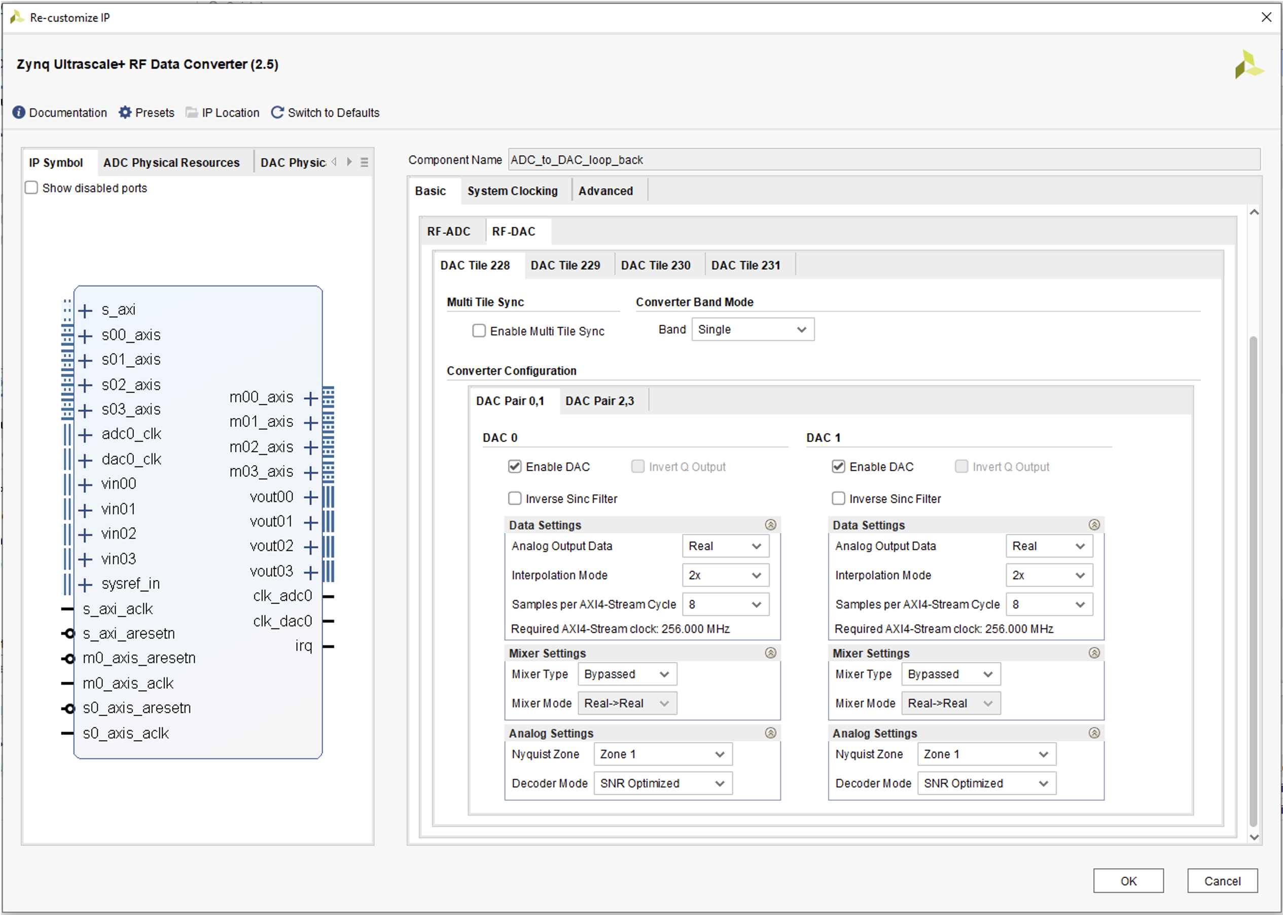
Figure 3: RF Data Converter DAC Tile
Data Settings:
- Analog Output Data = Real
- Interpolation Mode = 2x
- Samples per AXI4-Stream Cycle = 8
Required AXI4-Stream clock: 256MHz (will automatically be generated based on the system clock that is chosen for the DAC tile)
Mixer Settings:
- Mixer Type = Bypassed
- Mixer Mode = Real -> Real
Analog Settings:
- Nyquist Zone = Zone 1
- Decoder Mode = SNR Optimized
Apply the same settings for DAC Pair 0,1 and DAC Pair 2,3.
System Clocking
Figure 4 shows system clocking setting. ADC is sampled at 2.048GSPS, this will dictate AXI4-stream clock. Since samples per AXI4-Stream clock is 8 and decimation mode is 1, divide 2.048GSPS by 8x1 will result in 256MHz. Similarly, DACs analog output data is sampled is 4.096GSPS, samples per AXI4-Stream clock is 8 and interpolation mode is 2, the required AXI4-Stream clock is, 4.096GSPS divided by 8x2, 256MHz.
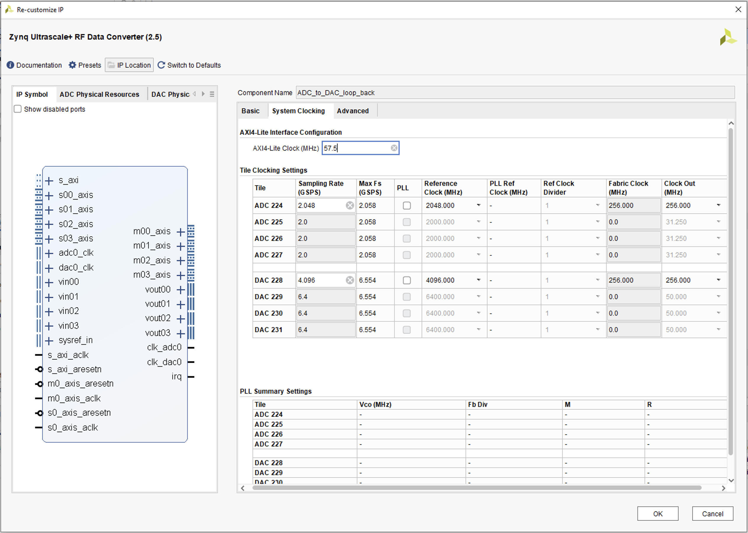
Figure 4: System Clocking
ADVANCED
Under advanced tab enable RF analyzer by selecting Enabled under drop-down menu.
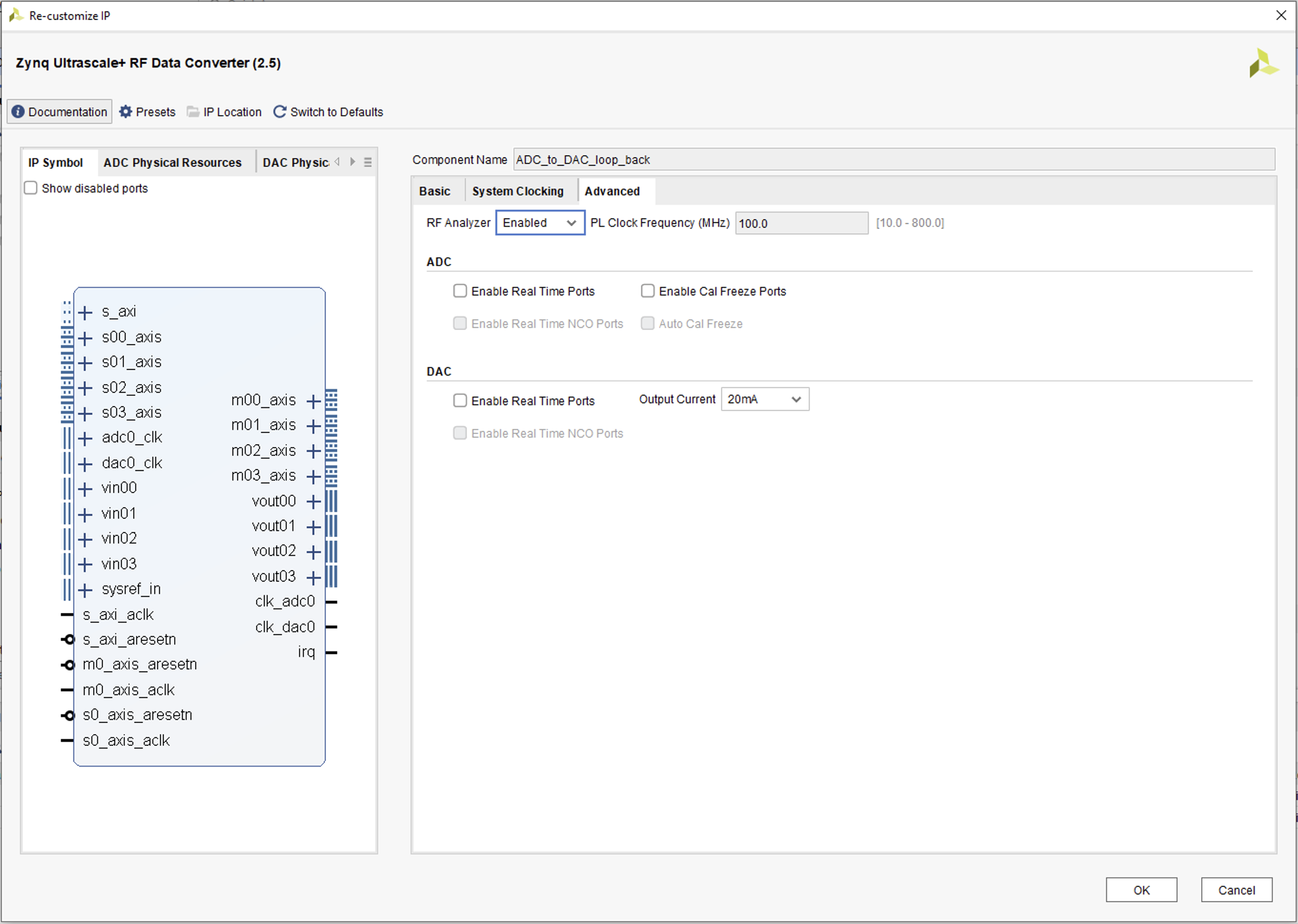
Figure 5: Enable RF Analyzer
Once we create a Vivado project with the above-mentioned IP configuration settings we can right click on the system design and open an example project. Vivado will create an example project for you to test the loop back configuration. Figure 6 shows the ADC to DAC loop back design. Vivado will create the necessary constraint file and simulations sources. Now we can generate the bitstream. Once bitstream is generated, we have everything we need to use RF analyzer.
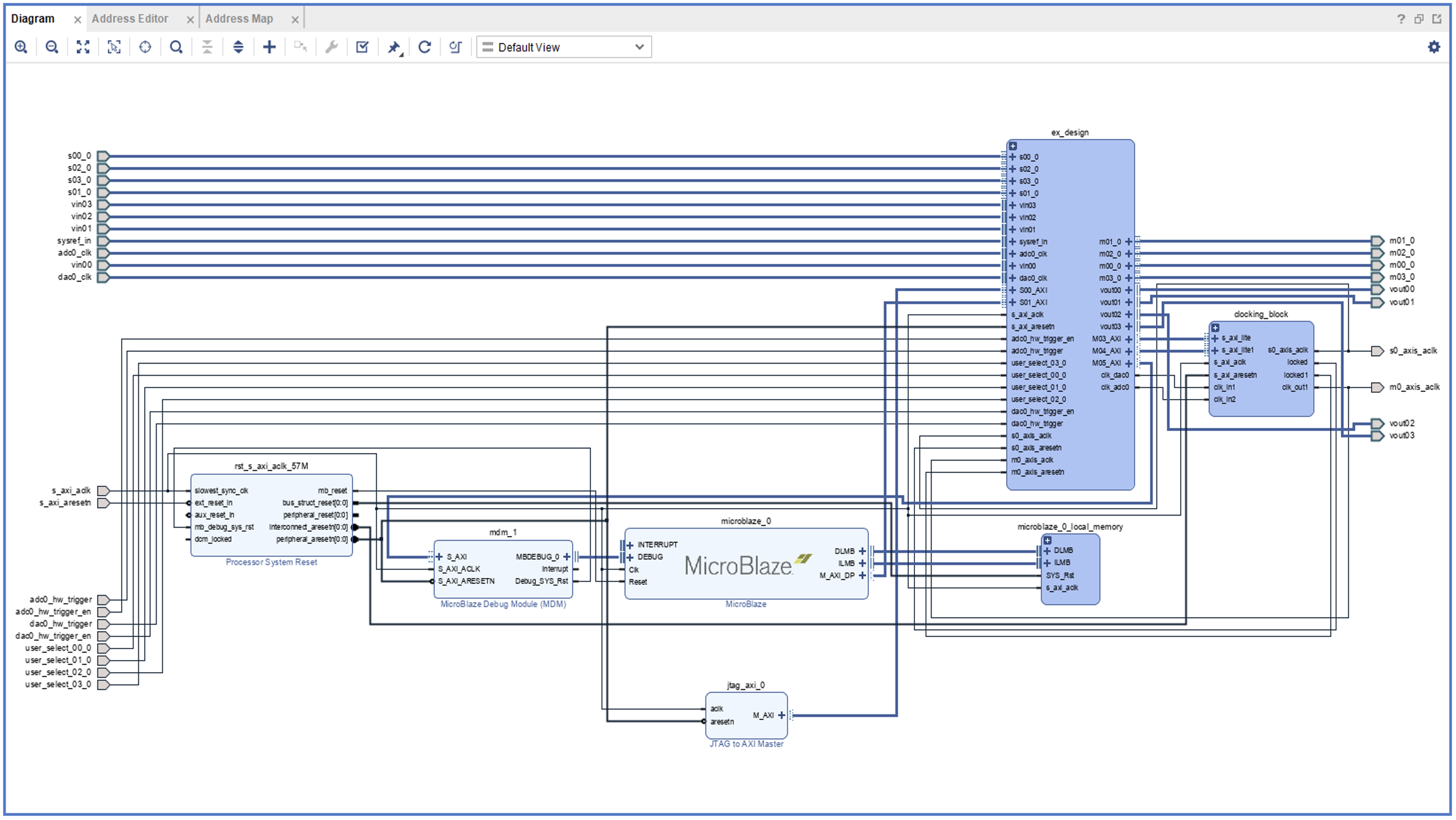
Figure 6: RFSoC ADC to DAC Loop Back Design
Board Connections
From Figure 1, we can see that the RF-ADCs and RF-DACs are present to the right side of the board. The pins connections to the board are shown in Figure 7.
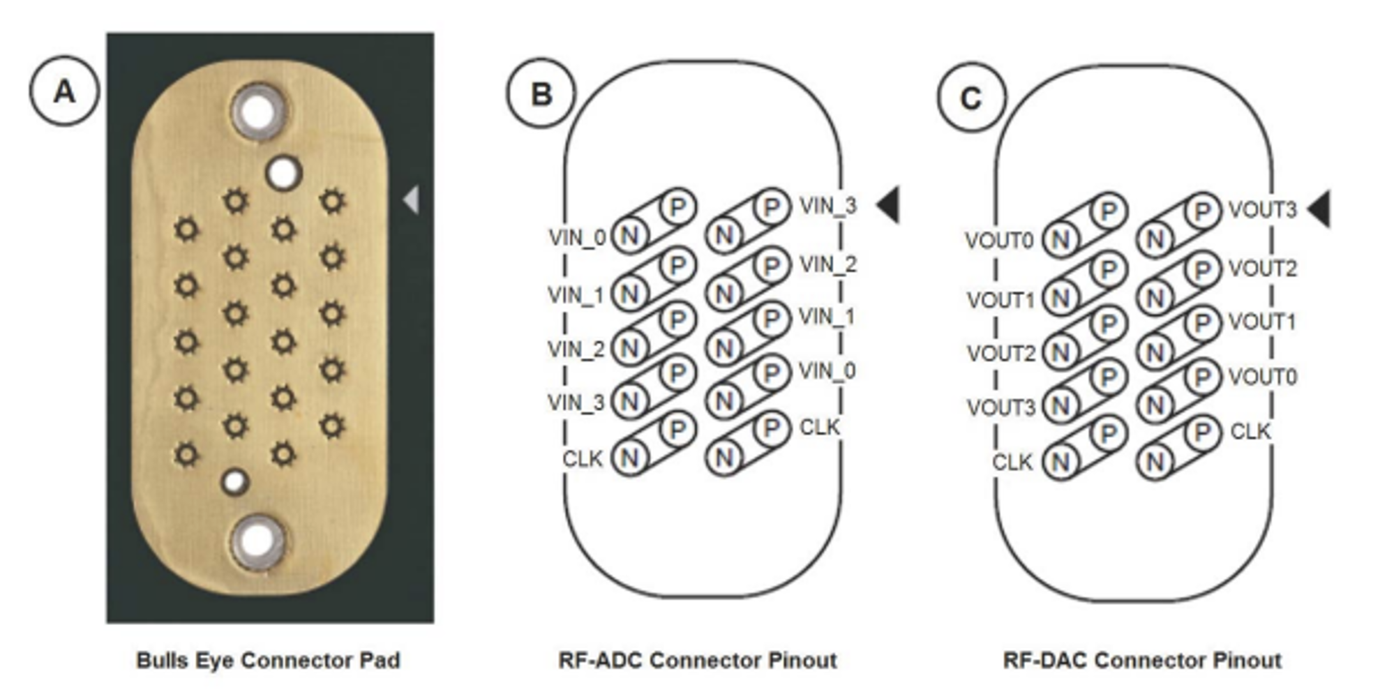
Figure 7: A: Bulls Eye Connector Pad; B: RF-ADC Connector Pinout; C: RF-DAC Connector Pinout
Use the given bulls eye cables to connect the RF-ADC and RF-DAC. Bulls eye cable is shown in Figure 8. Connect the flat end of the bullseye cable to the board.
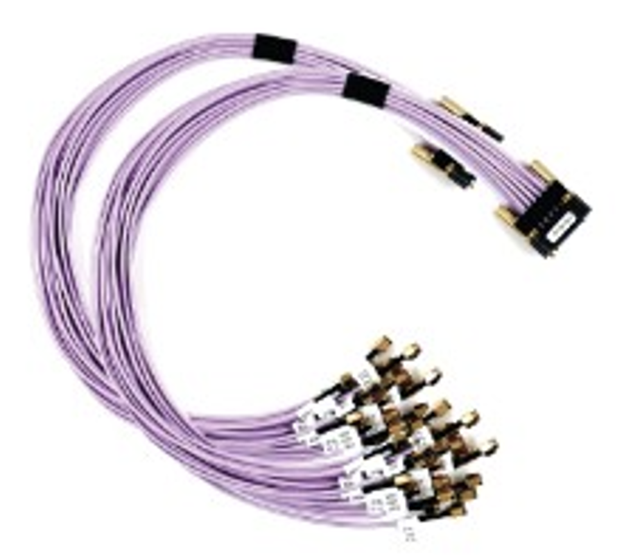
Figure 8: Bulls Eye Cable
Connect the ADC’s vin_0 pins p and n to DAC’s vout_0 pins p and n.
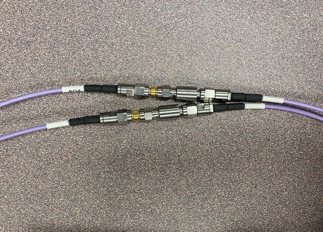
Figure 9: RF-ADC’s P and N pins connected to RF-DAC’s P and N pins
This will establish a loop back connection from RF-ADC to RF-DAC as intended from our design example. Clock pins for RF-ADC is connected to SuperClock-RF2 module callout pin 3 which can be seen in Figure 11, Figure 12 and Table 1. Similarly, RF-DAC’s clock pins are connected to the callout pin 1 which can be referred in Figure 11 and Table 1.
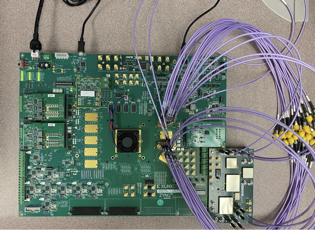
Figure 10: Board Connection
SuperClock-RF2 Module
Connect a JTAG cable and UART cable to the board. JTAG connection will to load the bitstream and UART will load the clock files to SuperClock-RF2 module. In other words, RF analyzer communicates with the board using JTAG cable and System Controller connects the board using UART cable.
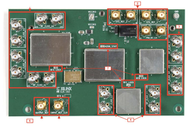
Figure 11: SuperClock-RF2 Module
For the example design will be using on board clocks generated from the SuperClock-RF2 module shown in Figure 11. SuperClock-RF2 module connects to the clock module interface and provides a programmable, ultra-low noise and low-jitter wideband RF clock source required for the RF data converters.
| Callouts | Feature Description |
|---|---|
| 1 | PLL A RF sampling clock SMA pairs |
| 2 | General-purpose clock SMA pairs |
| 3 | PLL B RF sampling clock SMA pairs |
| 4 | PLL C RF sampling clock SMA pairs |
| 5 | External reference clock input |
| 6 | Single-ended reference clock output |
| 7 | PLL lock indicator LEDs |
PLL A
PLL A has four differential output SMA pairs which are used as RF sampling clocks for RF-ADCs. Maximum frequency to which it can be programmed is up to 4.0 GHz. For our design will program it to 2.048 GHz.
PLL B and C
PLL B and C have two differential output SMA pairs that is used to program the RF-DACs sampling clocks. Maximum programmable frequency is up to 6.4 GHz. For our example design will program it to 4.096 GHz.
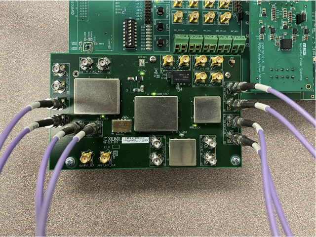
Figure 12: SuperClock-RF2 Module with connections
System Controller
Xilinx system controller is an application that runs on Zynq-7000 SoC at power up on the ZCU1275 board (Zynq UltraScale+ RFSoC 1275 Characterization board). This application is used to generate the required clocks to RF-ADCs and RF-DACs by configuring the SuperClock-RF2 module. Upon launching the application, you will be greeted with the board information window shown in the Figure 13.
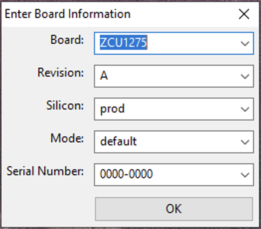
Figure 13: System Controller
After entering the board information and pressing OK, the main window of the system controller opens which is shown in Figure 14. On the left-hand side is the system controller controls and on the right side is a log of the operation. The necessary clock files can be downloaded from the user guide UG1285.
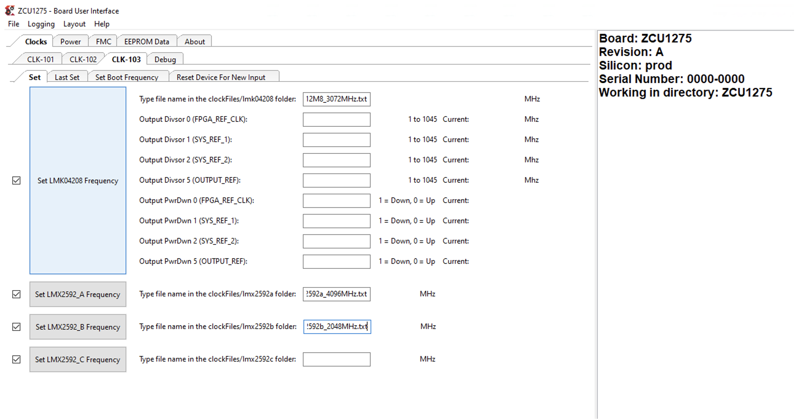
Figure 14: CLK-103 Set LMK***** Frequencies
Under clocks tab select CLK-103 tab because is the HW that is available on the board as it can be seen in the Figure 11 and Figure 12.
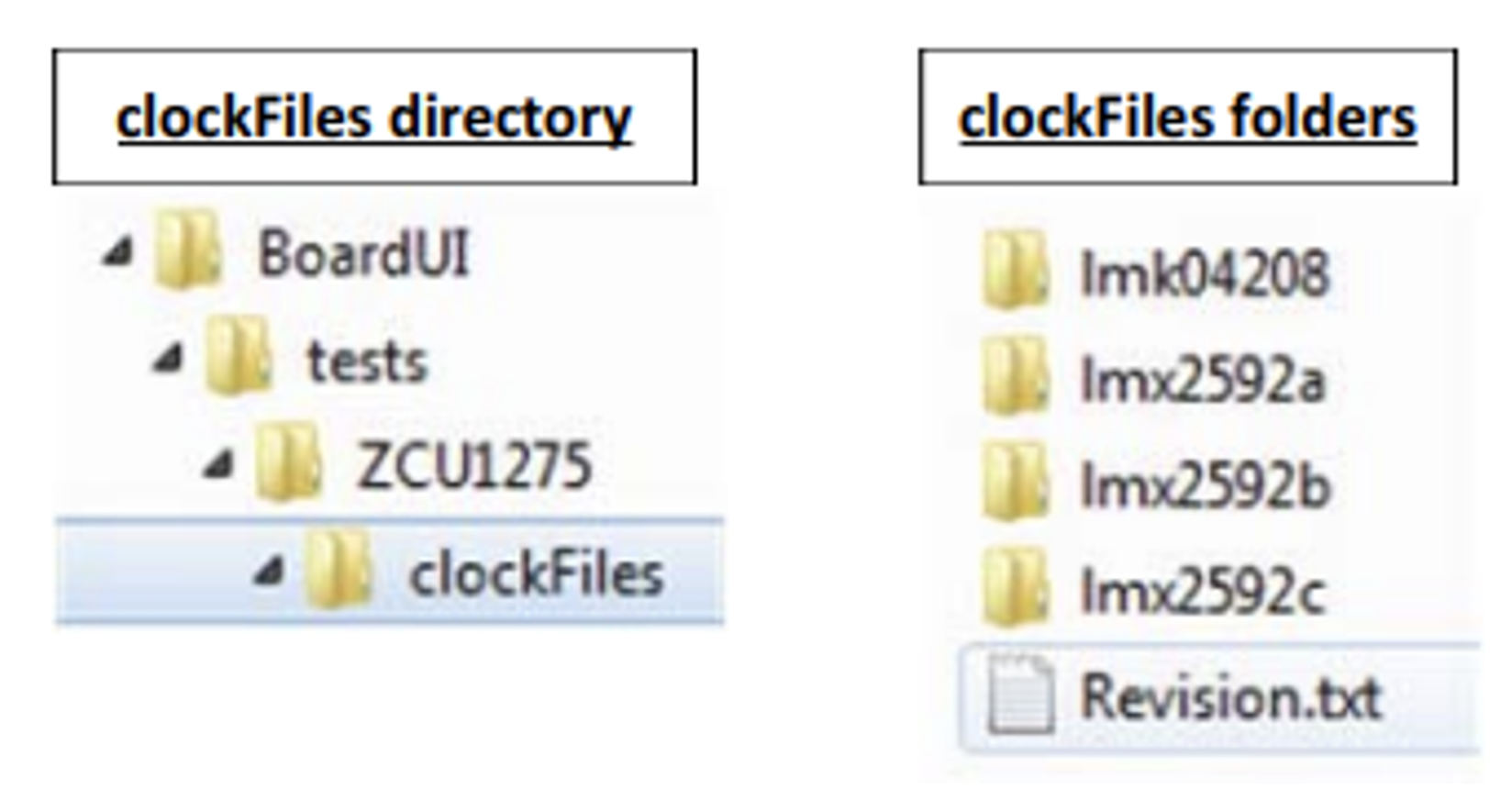
Figure 15: CLK-103 Clock Files
From the clock files directory select the correct clock files to load the correct clock files from the folders as shown below. It is important to include the complete name including the extension such as *.txt.
- CLK-103 LMK04208 Frequency: LMK04208_CLKin1_12M8_3072MHz.txt
- CLK-103 LMX2592 PLL A : LMX2592a_4096MHz.txt
- CLK-103 LMX2592 PLL B : LMX2592b_2048MHz.txt
Clicking on the set frequency tab will program the SuperClock-RF2 module present on the board with the required RF-sampling clocks. Along with the finished log report the LED indicators present on the SuperClock-RF2 module will light up indicating the process has completed successfully along with the finished message in the log window as shown in Figure 16.
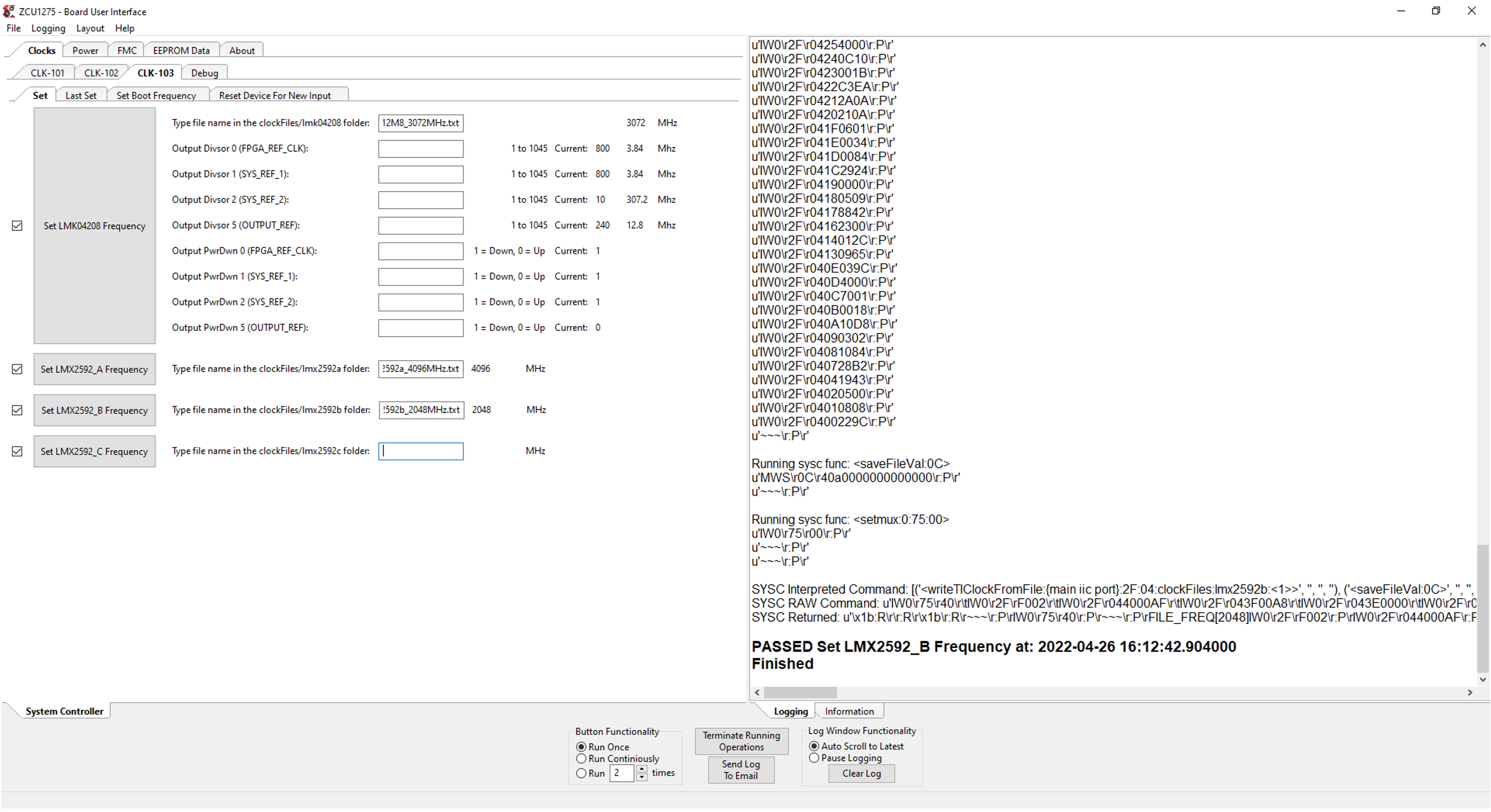
Figure 16: CLK-103 Set LMK***** Frequencies Log Report
RF Analyzer
Now that we have turned on our board and configured the necessary RF-sampling clocks we can start the RF analyzer application shown in Figure 17. On the starting window select the local server (target is on local machine) under connection. Under hardware highlight the detected board, in our case it the ZCU1275. Now point to the bitstream path that we generated using the example the design and click on Download Bitstream. This will configure the board with the loaded bitstream and activated the RF-ADCs and RF-DACs as intended while configuring the RF Data Converter IP.
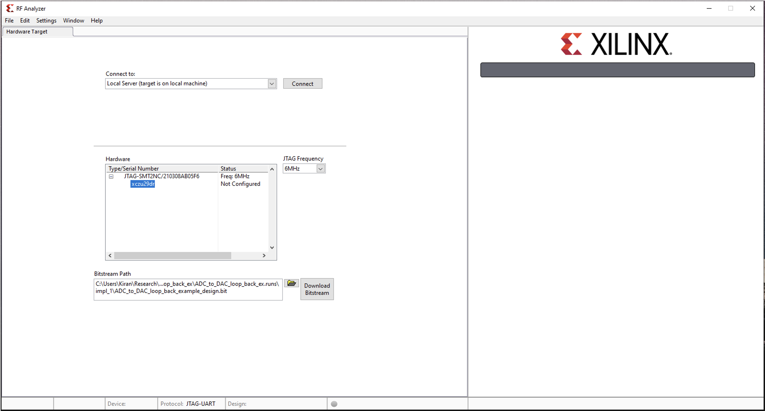
Figure 17: RF Analyzer
Active ADC and DAC tile will be highlighted in green as shown in Figure18.
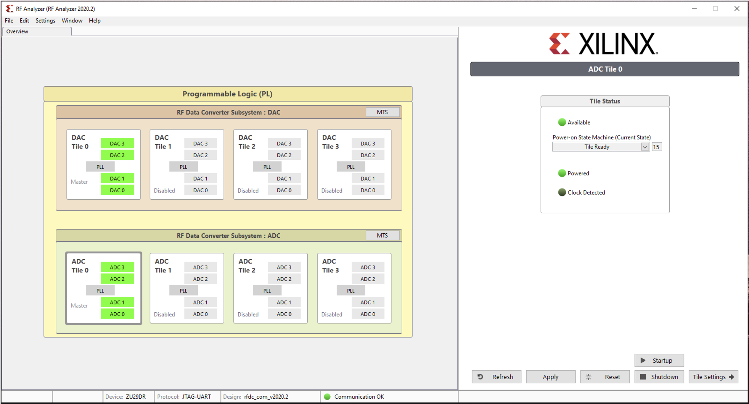
Figure 18: Active RF-ADC and RF-DAC Tiles
Select the RF-ADC/RF-DAC tile and set up the PLL reference clock. ADC Tile 0 – PLL and DAC Tile 0 – PLL clocking reference is set to 256MHz. This is AXI4-Stream clock that was generated automatically when configuring the RF Data converter IP.
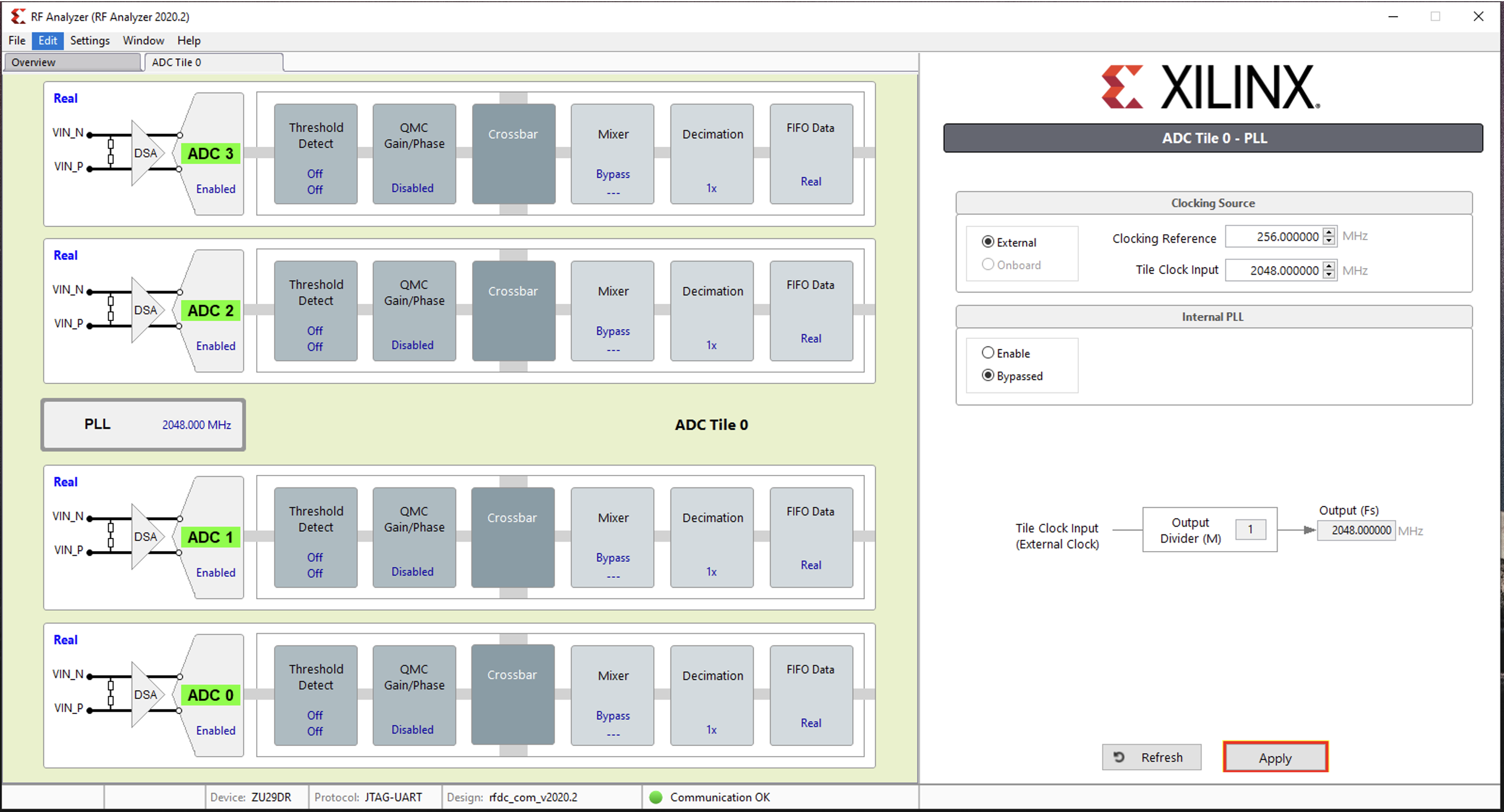
Figure 19: PLL Reference Clock for RF-ADC
The PLL clock reference for RF-ADC and RF-DAC is shown in Figure 19 and 20 respectively.
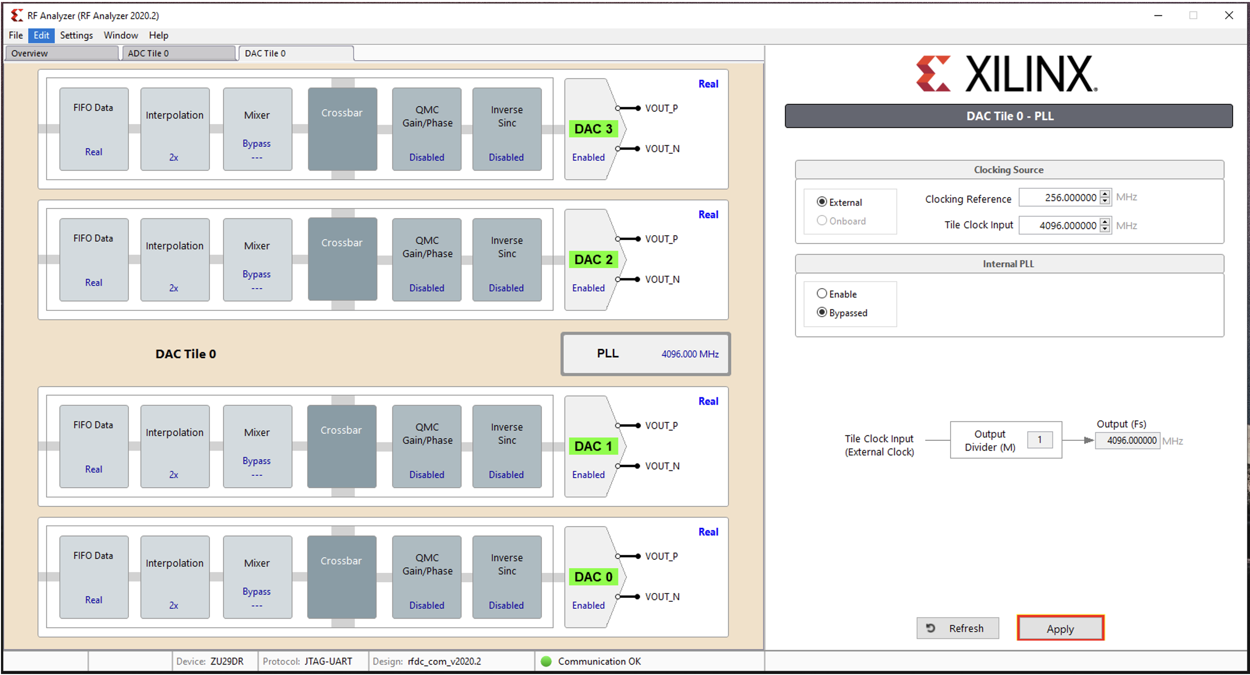
Figure 20: PLL Reference Clock for RF-DAC
Select DAC tile 0 to generate the analog signal. Figure 21 shows DAC tile configuration which should match the RF Data converter IP. Click on the generation button to start transmitting the analog output signal.
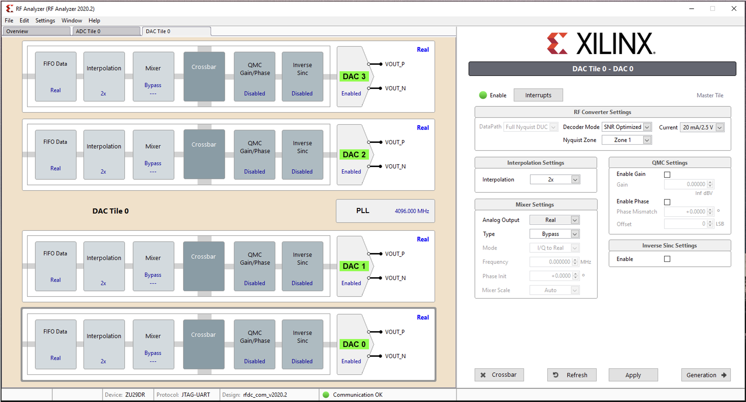
Figure 21: RF-DAC Tile Configuration
RF analyzer GUI will show the analog and the FFT plot of the generated signal as shown in the Figure 22 and Figure 23 respectively. User can choose a desired frequency to generate by changing the frequency value under the CF (center frequency) dialog box.
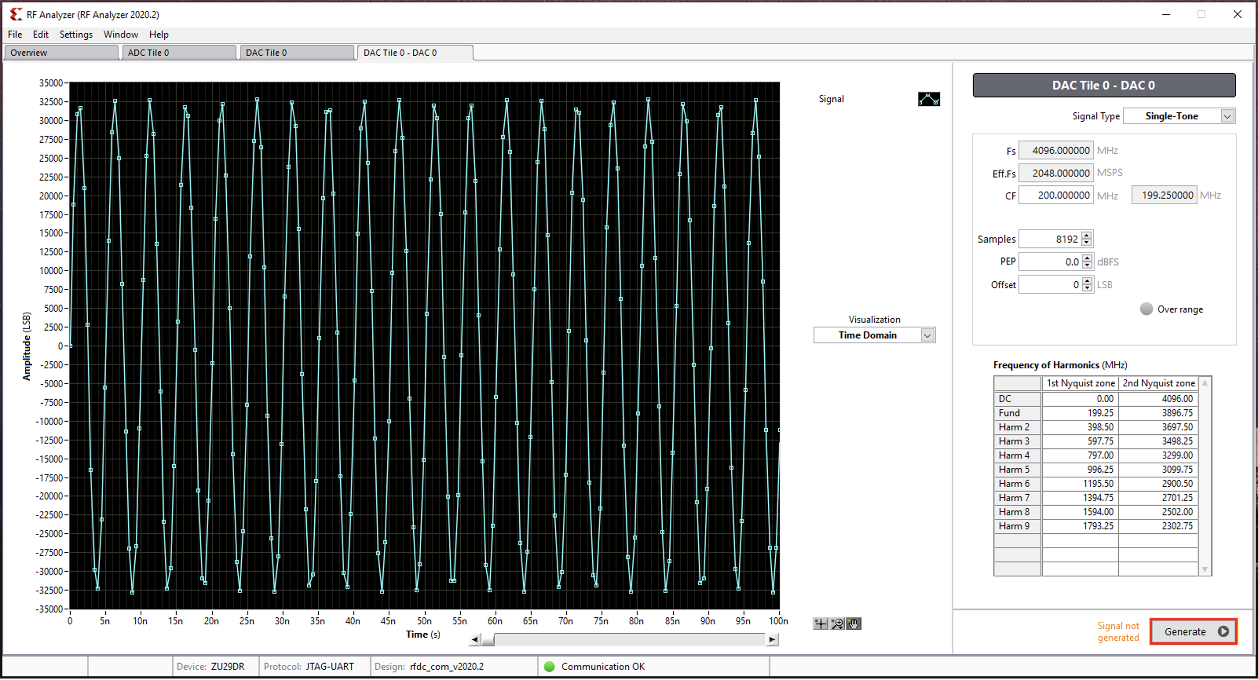
Figure 22: RF-DAC Tile: Time Domain Analysis
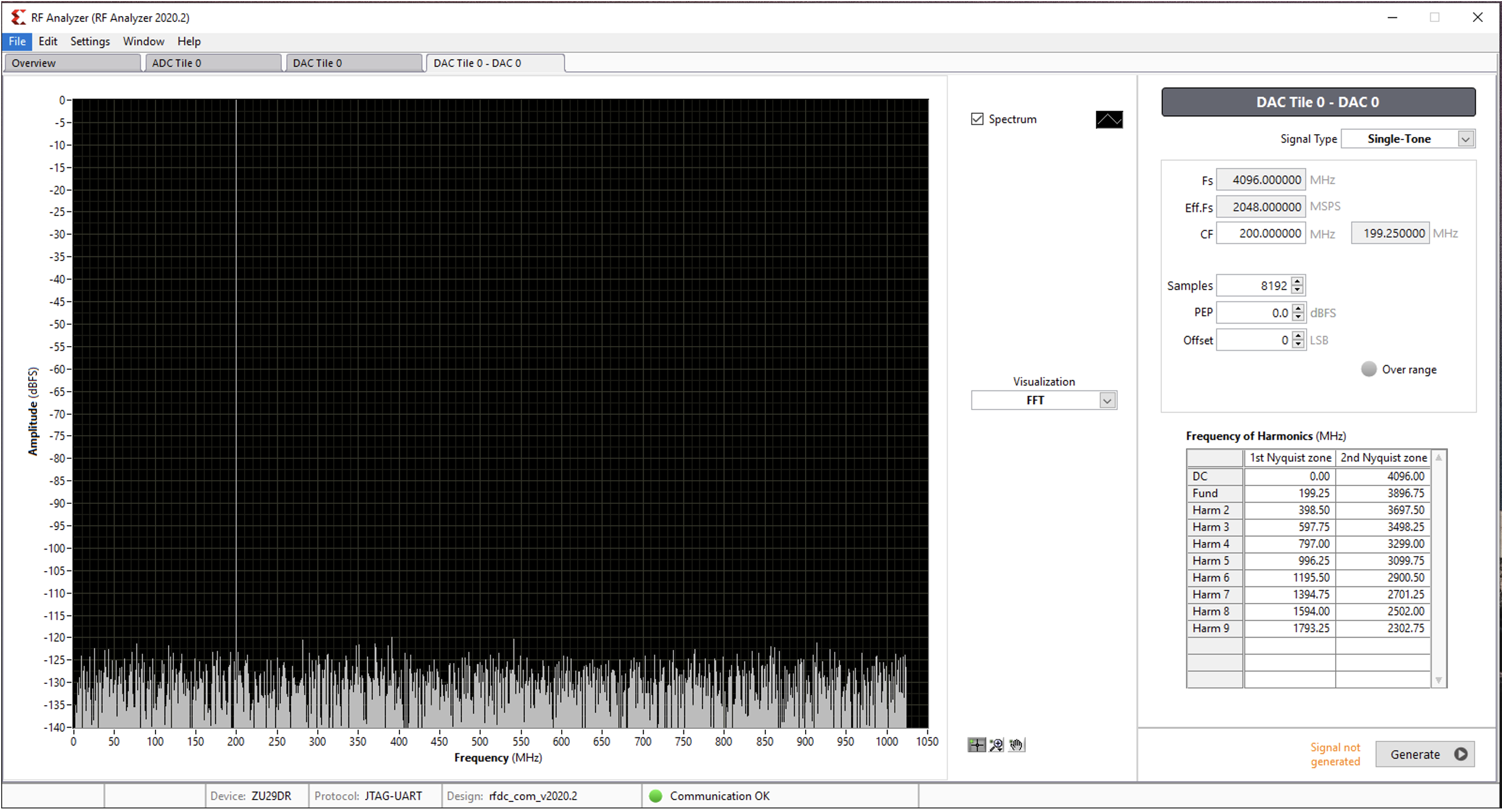
Figure 23: RF-DAC Tile: Frequency Domain Analysis
Once the analog is generated using the RF analyzer move back to the ADC tile tab and select the ADC 0. With configuration shown in the Figure 24 click on the acquisition button to capture the signal that is being generated from the RF-DAC.
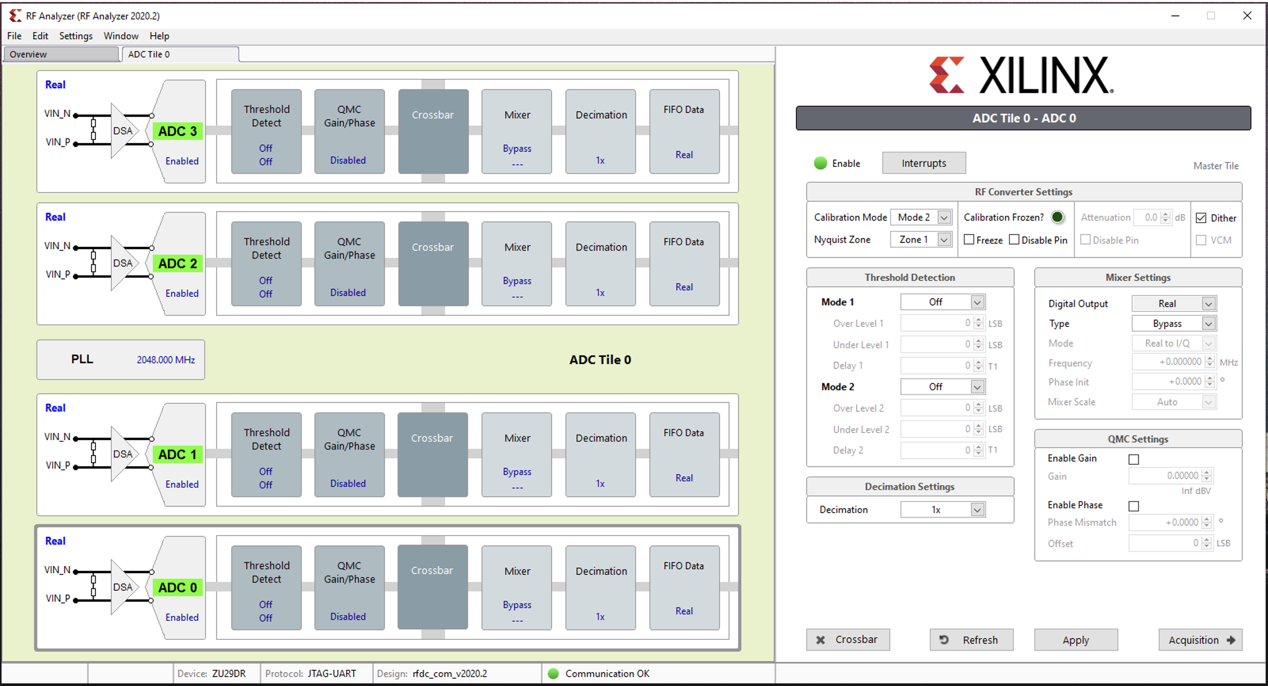
Figure 24: RF-ADC Tile Configuration
These tiles (ADC and DAC) should match the setting used in the RF data converter IP. RF analyzer will open another tab with the acquired signal as seen in Figure 25. Users can view the signal in both time domain and in frequency domain of the captured signal with a click of a button. Figure 25 and Figure 26 shows the captured signal by the RF-ADC tile in time domain and frequency domain respectively.
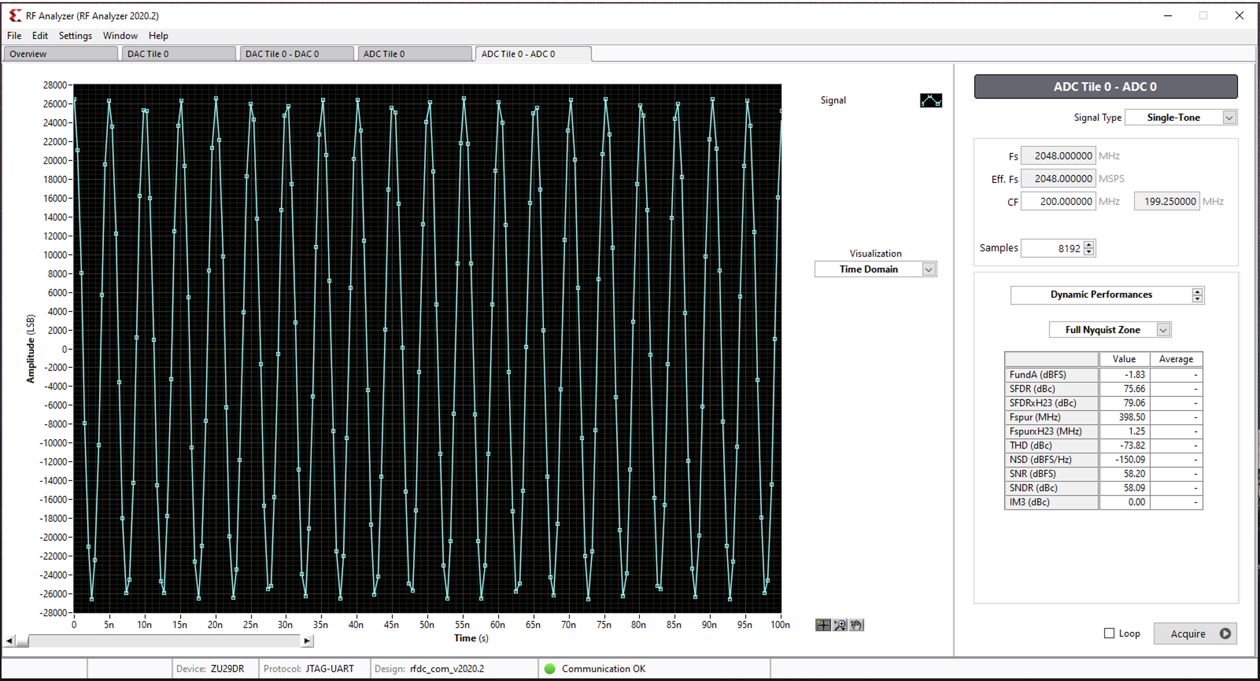
Figure 25: RF-ADC Tile: Time Domain Analysis
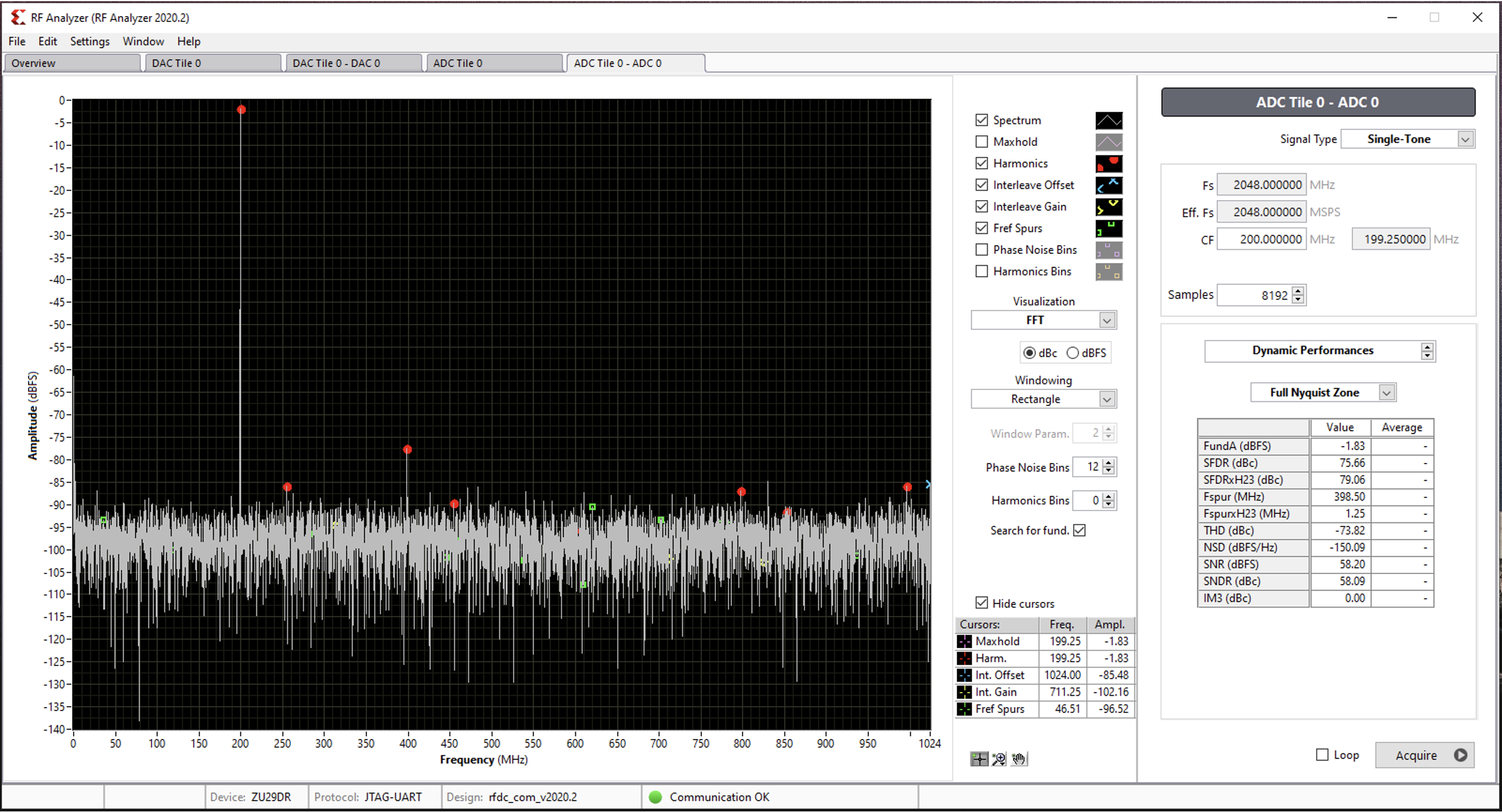
Figure 26: RF-ADC Tile: Frequency Domain Analysis
RF analyzer tool is an extremely useful tool in debugging the design. It also provides additional information such as harmonics, dynamic range, noise band, etc. The tool can also write the captured data to an excel sheet or to a text file for external use.